Download this article in PDF format.
The global semiconductor shortage has opened the door for criminals who want to cash in on the scarcity of these valuable components. According to the Wall Street Journal, this has pushed some buyers to take risks that they may not have even considered before.
“Dubious sellers are buying ads on search engines to lure desperate buyers. Sales of X-ray machines that can detect fake parts have boomed,” the publication reports. “It is a quality-control crisis created by the world’s scramble to land hard-to-find semiconductors at any cost. Without those essential parts, makers of products as varied as home appliances and work trucks are stuck in neutral as the global economy ticks back to life.”
The potential hazards associated with counterfeit chips have some organizations scrambling to find a resolution to the counterfeit boom. The National Institute of Standards and Technology (NIST), is one such organization that recently demonstrated a method that could electronically authenticate products before they leave the factory.
Using a technique called “doping,” NIST scientists use small clusters of “foreign” atoms of a different element from those in the device. Those foreign atoms are implanted just beneath the surface and alter the electrical properties of the topmost layer without harming it, creating a unique label that can be read by an electronic scanner.
The use of doping to create electronic tags for devices is not a new idea, but NIST says that its technique uses the sharp tip of an atomic force microscope (AFM) probe to implant atoms. This is simpler, less costly and requires less equipment than other doping techniques using lasers or a beam of ions, said NIST researcher Yaw Obeng, who represented the work in September at the International Conference on IC Design and Technology in Dresden, Germany.
"We're putting a sticker on every device, except that the sticker is electronic and no two are identical because in each case the amount and pattern of the dopant atoms is different," said Obeng, in NIST’s “Implanted atoms create unique electrical IDs that distinguish bona fide devices from forgeries.”
Laying Down the Foundation
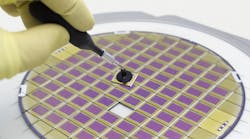
To create the electronic ID, scientists first deposited a 10-nanometer (billionth of a meter) film of aluminum atoms into 10-centimeter-square silicon wafers that were then broken into postage-stamp-size fragments so that they could fit in the AFM. The team then used the needle-like tip of the AFM probe to push aluminum atoms a few nanometers into the silicon fragments. The NIST says that the diameter of the implanted regions was tiny, no larger than 200 nm
NIST researchers also developed a new low-cost process for creating unique and non-duplicable ID tags by altering the electronic structure of silicon. These tags could be embedded into a device during the manufacturing process and easily authenticated by anyone receiving the device, ensuring a secure supply chain for components in critical systems.How it Works to Thwart Counterfeiting
The implanted atoms alter the arrangement of silicon atoms just beneath the surface of the wafer. These silicon atoms, as well as those that reside throughout the wafer, are arranged in a repeating geometric pattern known as a lattice. Each silicon lattice acts like an electrical circuit with a certain impedance, the AC (alternating current) equivalent of resistance in a DC (direct current) circuit, according to the NIST.
The lattice can serve as a distinctive electronic label—a nanometer-scale version of a QR code for the wafer. That way, when a scanner directs a beam of radio waves at the device, the electrically altered lattices respond by emitting a unique radio frequency corresponding to their impedance.
Counterfeit devices could be easily identified because they would not respond to the scanner in the same way. "This research is key,” said one NIST researcher, “because it offers a means to uniquely identify components by a secure, unalterable and inexpensive means.”


